

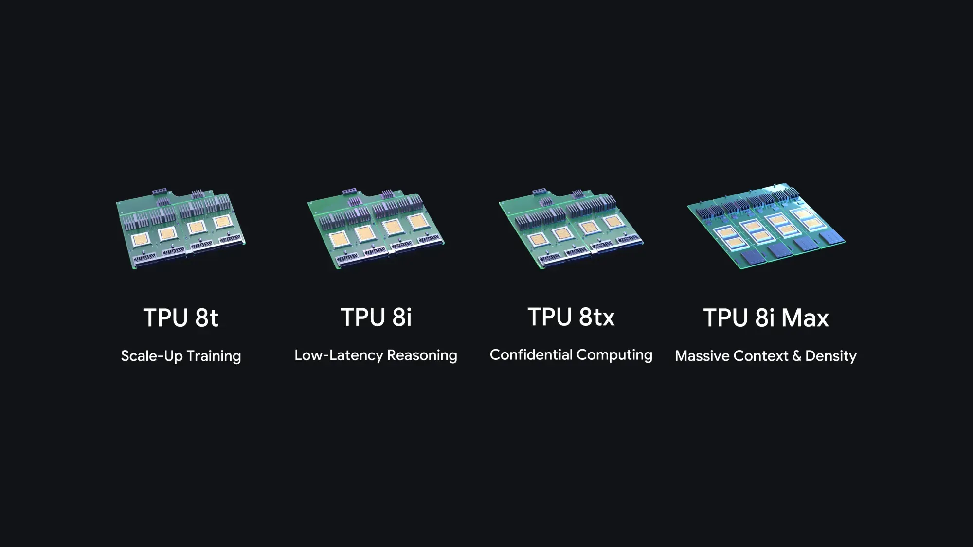
Google has expanded its eighth-generation Tensor Processing Unit portfolio with TPU 8tx and TPU 8i Max, two systems aimed at confidential AI workloads and memory-intensive agents. The additions bring the generation to four systems, alongside TPU 8t for large-scale training and TPU 8i for low-latency reasoning. Google has not specified pricing, supported regions, or a general availability date for either new system.
The key distinction is that TPU 8tx and TPU 8i Max are new system configurations built around existing silicon. Google says its modular architecture lets teams change packaging, memory, networking, and security without waiting for a full chip development cycle. TPU 8tx uses TPU 8t silicon, while TPU 8i Max combines two TPU 8i chips in a single package.
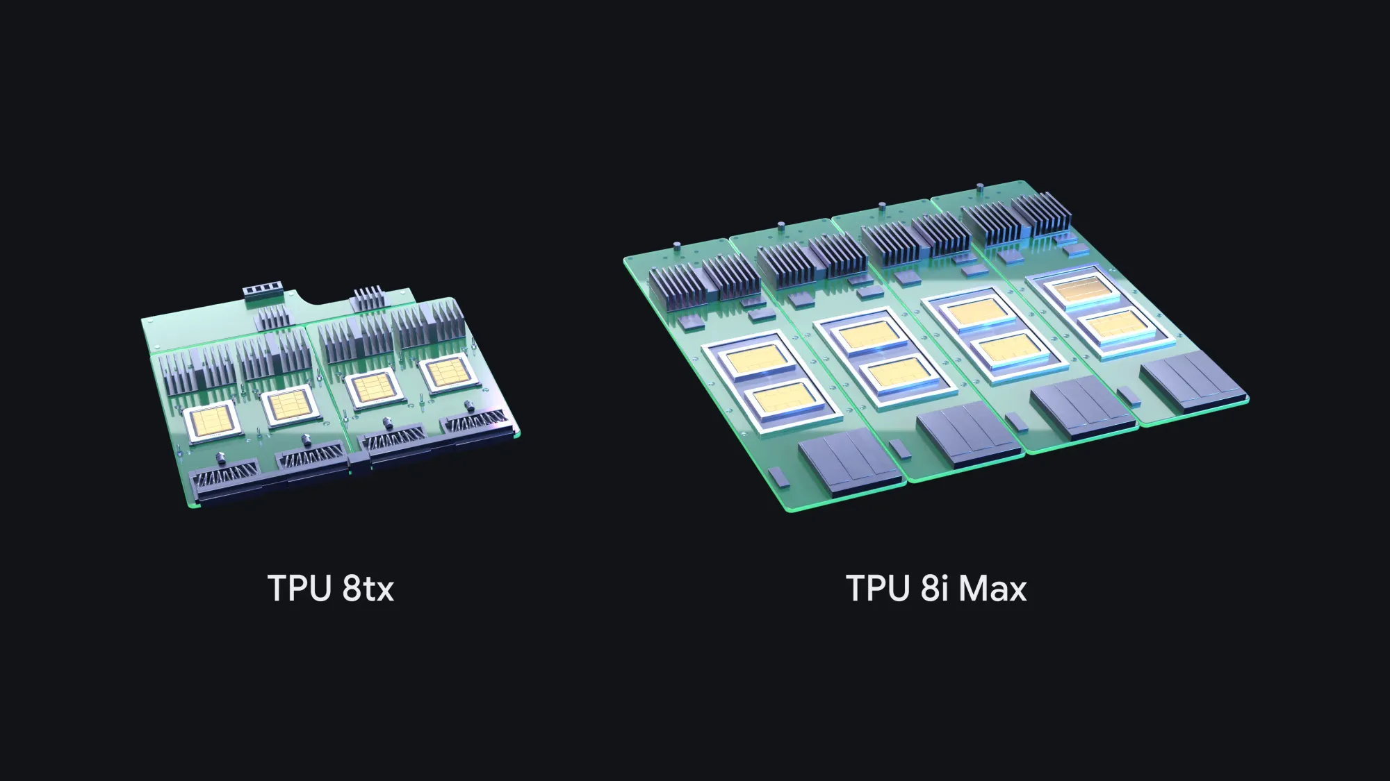
TPU 8tx targets regulated enterprises and governments running models and autonomous agents against sensitive information. It pairs TPU 8t silicon with custom AMD CPU hosts and adds hardware-level confidential computing to protect data and model weights during processing. This extends protection into active computation, beyond encryption during storage and network transmission.
The system also adopts the Boardfly network developed for TPU 8i. Google claims the combination delivers up to twice the performance of TPU 8t, with a near-zero performance penalty for its security capabilities. Alongside inference, TPU 8tx supports smaller training workloads, private fine-tuning, model distillation, and reinforcement learning. Organizations can perform these tasks on one system without transferring sensitive data between separate clusters.
TPU 8i Max addresses the memory demands of agents processing large codebases, lengthy videos, and million-token contexts. According to Google, its dual-chip package provides twice the compute, SRAM, and high-bandwidth memory bandwidth of TPU 8i. The company also says it places twice the silicon within the existing rack footprint, increasing compute density.
For comparison, Google’s previously published TPU 8i specifications list 288 GB of high-bandwidth memory, 384 MB of on-chip SRAM, and 8,601 GB/s of memory bandwidth. The new announcement specifies doubled SRAM and bandwidth for TPU 8i Max but does not provide an absolute HBM capacity figure for the new package.
Google is pairing the hardware expansion with software intended to make TPUs accessible through existing development tools. TorchTPU supports native PyTorch execution, with TPU backends for vLLM and SGLang. A TPU agent suite, available in preview, connects to Claude Code, Cursor, and Google Antigravity to assist with onboarding, performance diagnosis, and custom kernel tuning. Google also announced an open-source XLA Serving Engine for serving models through a low-latency C++ runtime across TPUs, GPUs, and CPUs.
Google TPU, video source - Google
Another component, Agent Compute Engine, suspends idle agent sessions and moves their working memory off the accelerator in milliseconds, Google says. It targets workloads that spend extended periods waiting for tools, database responses, or human input, leaving accelerator resources occupied between computation steps.
TPU Sync handles a related problem at the memory layer. Google describes it as a system connecting accelerator HBM, host DRAM, shared storage, and networking into a coordinated hierarchy. It moves KV caches, the stored attention state used during model inference, between memory tiers. It also transfers context between separate prompt-processing and token-generation nodes and synchronizes weights for reinforcement learning. Google claims reductions of more than 90% in KV transfer latency and time to first token, although the supplied announcement does not detail the test conditions.
For cluster orchestration, Google says Cloud Pathways is now generally available on Google Kubernetes Engine. It brings the runtime used behind Gemini to Cloud customers, allowing multiple TPU slices to be managed through a single controller for pre-training, reinforcement learning, and inference. Its recovery features include replacing slices in under a minute and redistributing workloads across available hardware.
GKE dynamic slicing is also generally available, according to the announcement. It uses optical circuit switching to assemble TPU resources into larger configurations or divide them into smaller workloads. Google reports up to five times faster job startup and up to 4.5 times faster fault recovery. The company also claims leading price-performance results on InferenceX and AgentX using its native vLLM-TorchTPU stack, though it did not include numerical results in the supplied text.
Google developed its first TPUs more than a decade ago for internal workloads such as voice recognition and translation. The accelerators now support Gemini training and serving, Google Cloud workloads, and customer data center deployments. According to Amin Vahdat, Google’s chief technologist and senior vice president for AI and Infrastructure, the TPU business has nearly 100 customers across frontier AI labs, financial firms, retailers, and universities. The expanded portfolio reflects that broader customer base, with separate configurations for training, reasoning, confidential computation, and large-context processing.
Sources and related context
- Google’s eighth-generation TPU architecture deep dive: Supports: Google’s specification table supports the baseline TPU 8i figures of 288 GB HBM, 384 MB SRAM, and 8,601 GB/s memory bandwidth used in the article’s comparison.
- Google announces native PyTorch inference engines for vLLM and SGLang on TPU: Supports: The announcement supports the article’s description of TorchTPU-based vLLM and SGLang backends and TPU Sync transfers for tiered KV caches and separate prefill and decode hosts.


